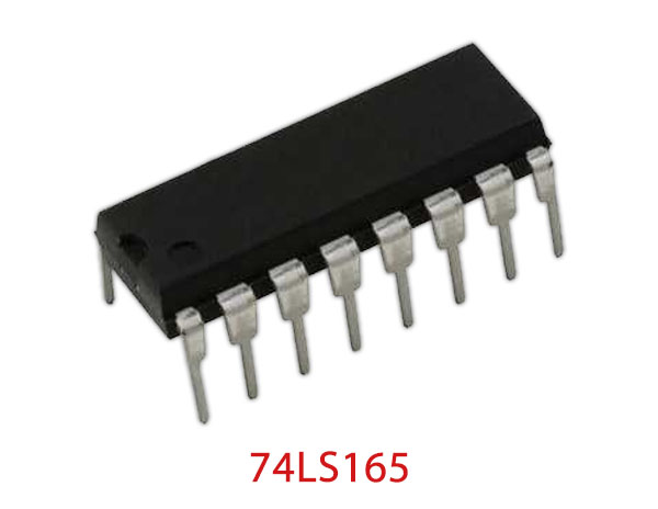
The 74LS series of integrated circuits (ICs) was one of the most popular logic families of transistor-transistor logic (TTL) logic chips. 74LS series is a bipolar, low-power Schottky IC.The 74LS165A is an 8-bit serial shift register that shifts the data in the direction of QA toward QH when clocked. Parallel-in access to each stage is made available by eight individual, direct data inputs that are enabled by a low level at the shift/load (SH/LD\) input.

74LS165 Features
- 8-Bit Shift Register which Shifts Data from Qa to Qh when Clocked
- Complementary Outputs
- Gated Clock Inputs
- Clock Frequency up to 35MHz
- Standard TTL Switching Voltages
74LS165 Specifications
| Supply Voltage | 4.75 – 5.25Vdc |
| Maximum Clock Frequency | 40Mhz |
| Power Dissipation | 2mW/gate @100kHz |
| Minimum Output Current | 8mA |
| Propagation Delay | 10nS |
| Fan Out (TTL Loads) | 20 |
74LS165 Pinout Diagram

74LS165 Pin Description
| Pin No | Pin Name | Description |
| 1 | PL’ | Asynchronous Parallel Load (Active LOW)Input |
| 2 | CP1 | Clock (LOW-to-HIGH Going Edge) Input |
| 3 | P4 | Parallel Data Input |
| 4 | P5 | Parallel Data Input |
| 5 | P6 | Parallel Data Input |
| 6 | P7 | Parallel Data Input |
| 7 | Q7′ | Complementary Output |
| 8 | GND | Ground |
| 9 | Q7 | Serial Output from Last State |
| 10 | DS | Serial Data Input |
| 11 | P0 | Parallel Data Input |
| 12 | P1 | Parallel Data Input |
| 13 | P2 | Parallel Data Input |
| 14 | P3 | Parallel Data Input |
| 15 | CP2 | Clock (LOW-to-HIGH Going Edge) Input |
| 16 | VCC | Positive Supply |
Applications
- The shift registers are used for temporary data storage.
- The shift registers are also used for data transfer and data manipulation.
- The serial-in serial-out and parallel-in parallel-out shift registers are used to produce time delay to digital circuits.
74LS165 Alternative Equivalent
74LS166
Download 74LS165 8-bit Serial Shift Register, Parallel Load Datasheet from the link given below.


